Paper on reversible photo-induced doping published in Nanoscale.
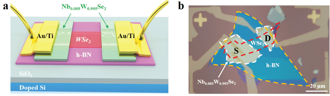
We report a reversible photo-induced doping effect in two-dimensional (2D) tungsten diselenide (WSe2) field effect transistors on hexagonal boron nitride (h-BN) substrates under low-intensity visible light illumination (∼10 nW μm−2). Our experimental results have shown that this reversible doping process is mainly attributed to two types of defects in h-BN substrates. Moreover, the photo-doped WSe2 transistors can be stable for more than one week in a dark environment and maintain the high on/off ratio (108) and carrier mobility, since there are no additional impurities involved during the photo-induced doping process to increase the columbic scattering in the conducting channel. These fundamental studies not only provide an accessible strategy to control the charge doping level and then to achieve a writing/erasing process in 2D transistors, but also shed light on the defect states and interfaces in 2D materials.