| Optoelectronics in 2D Materials |
|---|
High Performance Phototransistors
We report high-performance WSe2 phototransistors with two-dimensional (2D) contacts formed between degenerately p-doped WSe2 and undoped WSe2 channel. Studies have shown that the high photoresponsivity and short response time of our WSe2 phototransistor are mainly attributed to the lack of Schottky-barriers between degenerately p-doped WSe2 source/drain contacts and undoped WSe2 channel, which can reduce the RC time constant and carrier transit time of a photodetector. Our experimental results provide an accessible strategy to achieve high-performance WSe2 phototransistor architectures by improving their electrical transport and photocurrent generation simultaneously, opening up new avenues for engineering future 2D optoelectronic devices.
Wang, T., Andrews, K., Bowman, A.. Hong, T., Koehler, M,, Yan, J., Mandrus, D., Zhou, Z., and Xu, Y. Nano Lett. 18 (5), 2018.
Tu Hong, Bhim Chamlagain, Shuren Hu, Sharon M. Weiss, Zhixian Zhou, and Ya-Qiong Xu. ACS Nano 9(5), 2015.
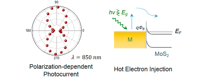
Photocurrent Generation in Metal-Semiconductor Junctions
When incident photon energy is above the direct bandgap of few-layer MoS2, the maximum photocurrent response occurs for the light polarization direction parallel to the metal electrode edge, which can be attributed to photovoltaic effects. In contrast, if incident photon energy is below the direct bandgap of MoS2, the photocurrent response is maximized when the incident light is polarized in the direction perpendicular to the electrode edge, indicating different photocurrent generation mechanisms. Further studies show that this polarized photocurrent response can be interpreted in terms of the polarized absorption of light by the plasmonic metal electrode, its conversion into hot electron–hole pairs, and subsequent injection into MoS2. These fundamental studies shed light on the knowledge of photocurrent generation mechanisms in metal–semiconductor junctions, opening the door for engineering future two-dimensional materials based optoelectronics through surface plasmon resonances.