| Contact Engineering in 2D Materials |
|---|

Andrews et al., ACS Nano, 2020.
2D Semiconductor Interlayer Contacts
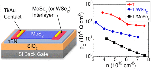
By inserting ultrathin 2D semiconductor interlayers at the contact interface the Schottky barrier Height (SBH) and contact resistivity of MoS2 field-effect transistors (FETs) can be minimized. This principle is demonstrated by inserting MoSe2 (WSe2) between the MoS2 channel and Ti electrodes to effectively reduce the SBH at the contacts from ~ 100 to ~ 25 meV, contact resistivity from ~ 6 x 10^{-5} to ~ 1 x 10^{-6} Ω⋅cm^{2}, and current transfer length from ~ 425 to ~ 60 nm. The drastic reduction of SBH can be attributed to the synergy of Fermi-level pinning close the conduction band edge of the MoSe2 interlayer and favorable conduction band offset between the MoSe2 interlayer and MoS2 channel. As a result of the improved contacts, MoS2 FETs with Ti/MoSe2 contacts also demonstrate higher two-terminal mobility.
Degenerately Doped 2D/2D Contacts
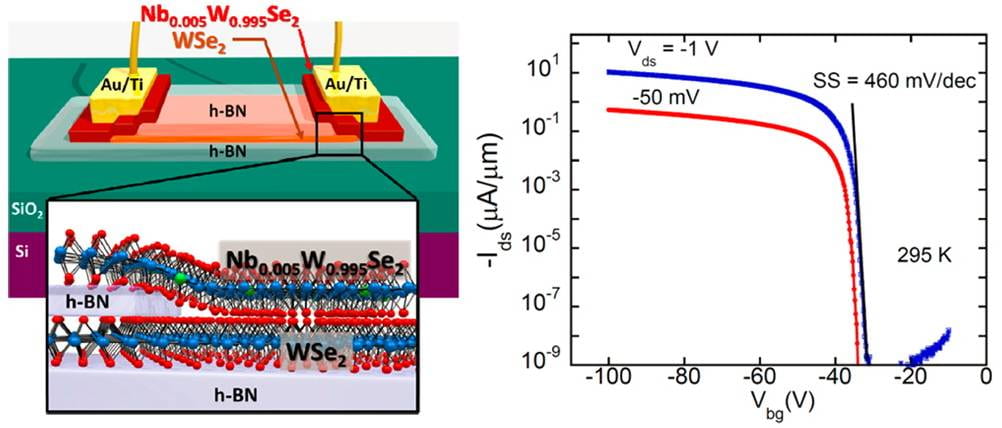
Making use of substitutionally doped TMDs as a drain/source contacts we can fabricate few-layer TMD field-effect transistors with 2D/2D contacts that exhibit low contact resistances of 0.3kΩ⋅μm, high on/off ratios up to >10^9, and high drive currents exceeding 320μAμm−1. These favorable characteristic allow us to reach a two-terminal field-effect mobility of approximately 200cm2V−1s−1 at room temperature, which increases to >2000cm2V−1s−1 at cryogenic temperautres in few-layer tungesten diselenide. This method is applicable to several other TMDs and two-dimensional materials.

Chuang et al., Nano Lett. 16 (3), 2016.


Highly Doped Graphene Contacts
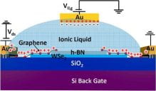
Using extremely large electric double layer capacitance of an ionic liquid gate one can minimize the Schottky barrier height by tuning the work function of graphene at the graphene/TMD interface within an enormously large range. As a result, we have formed formed for the first time, in a single device structure, tungsten diselenide field-effect transistors of both n- and p-type that display low-resistance contacts (down to ~ 2kΩ⋅μm) and a relatively high carrier mobility (>300cm2V−1s−1 at 77K).
Chuang et al., Nano Lett. 14 (6), 2014.


